Description
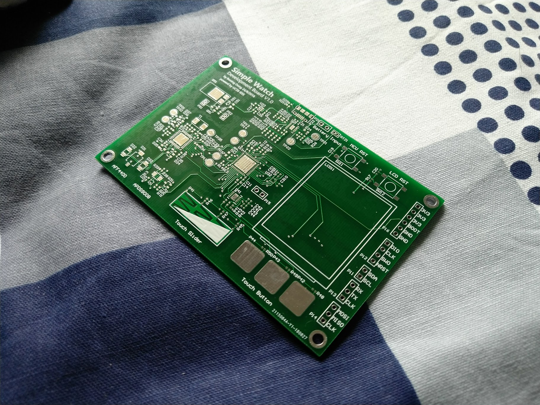
My initial purpose in starting this project is to polish my PCB designing and system design skills further. I purely want to work on something that requires a compact size and multi-layer ( more than two layers) PCB design. As its name indicates, I tried to build a “product level” smartwatch from scratch. According to my design, the watch will integrate a color LCD screen, capacitive touch interface, and capable of tracking users’ heart rate. So, even though the project name is called “simple watch,” the design and engineering procedures are actually not simple.
The whole project can be divided into the following phrases:
- planing the functionalities
- designing the hardware systems
- choosing the components
- designing, manufacturing and assembling the PCBs
- developing the firmware
Progress
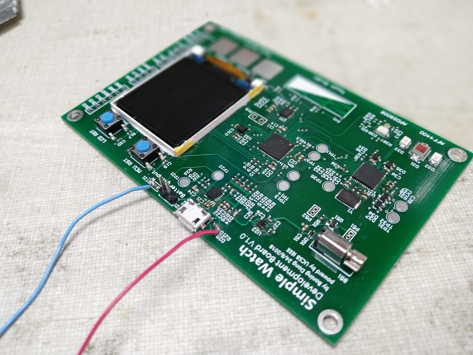
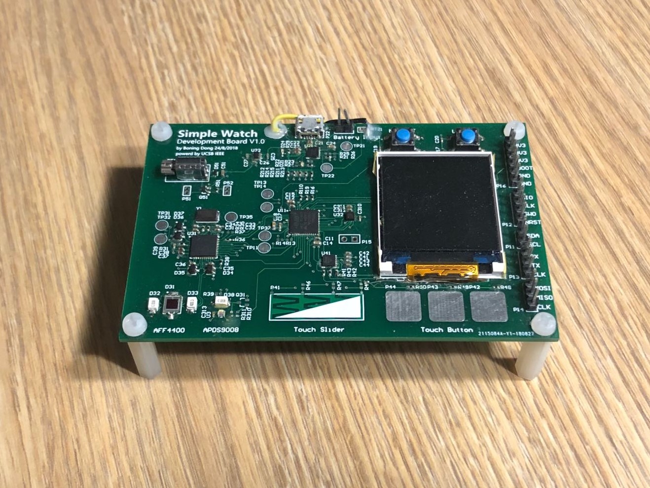
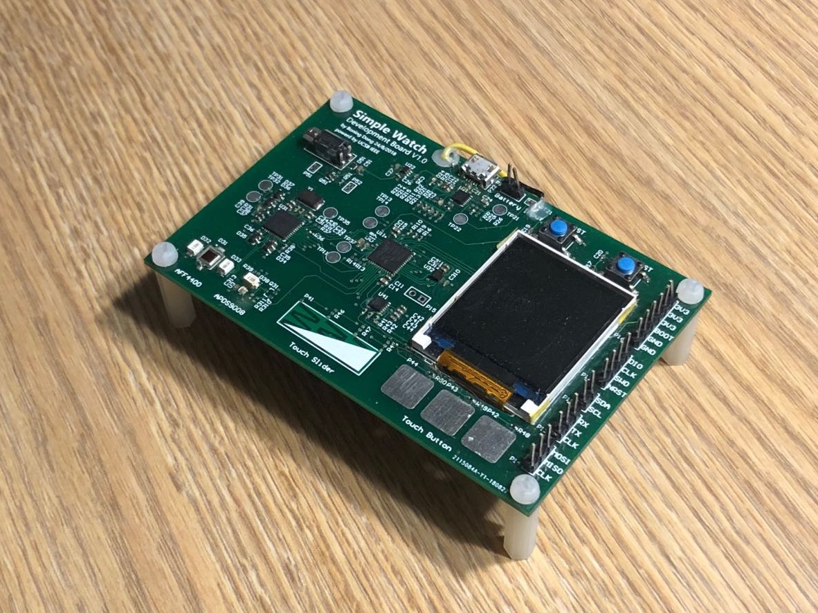
Currently, I finished designing and assembling the prototype board for developing firmware and validating my design. On the board, different subsystems are connected using 0 Ohm resistors, which eases the process of the board modularly. (Updated 07/28/2019)